RESEARCH
Introduction to Specialized Research Areas

RESEARCH

RESEARCH

Why do we learn?
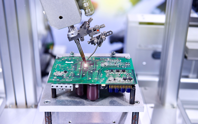
Each year, 40 students are admitted. The semiconductor industry is widely recognized as a key driver and technological enabler of the entire electronics value chain, and it is currently experiencing rapid growth. Taiwan plays a pivotal role in the global semiconductor supply chain. As production capacity continues to expand, the shortage of talent has become increasingly pronounced. This program is designed in response to the fast-paced development of the semiconductor era, with the goal of cultivating outstanding students equipped with comprehensive knowledge of semiconductors. The core research areas include IC fabrication, device innovation, chip design, and quantum physics.
From a silicon wafer to a packaged, marketable product, it is essential to first understand the fundamental knowledge of semiconductor devices and then learn the associated fabrication processes. These include photomask fabrication, photolithography, ion implantation, thermal diffusion or annealing, chemical vapor deposition or physical film deposition, dry and wet etching, as well as chemical mechanical polishing and device packaging. Through this curriculum, students gain a comprehensive understanding of the pivotal role semiconductors play in modern technology.
From the currently prominent metal-oxide-semiconductor field-effect transistors (MOSFETs) to the latest quantum computing units, the application of cutting-edge physical theories to pioneer unprecedented new devices has continually driven groundbreaking revolutions in the semiconductor industry.


Chips are designed with different architectures according to various application requirements, using logic gates to establish connections between components. In addition to simulating the efficiency of interactions among circuit elements, energy interference between systems is also an important issue to be considered.
As semiconductor devices continue to scale down, macroscopic physics is no longer adequate for analysis, and quantum physics has become a fundamental cornerstone of emerging semiconductor solid-state theories.
Why do we learn?
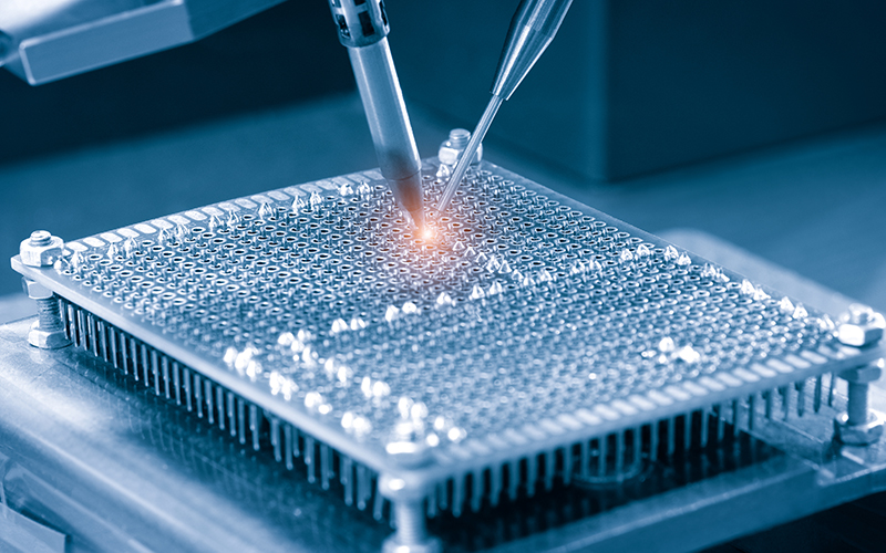
Each year, 25 students are admitted. The program aims to cultivate outstanding students with cross-disciplinary learning abilities. Rather than focusing on a single field, interdisciplinary study provides an informational advantage by integrating knowledge from related areas. During the first and second years, students complete fundamental required courses in mathematics, physics, chemistry, electronics, materials science, and programming (including laboratory courses). Beginning in the third year, students may select two core areas of study based on their personal interests. The four major fields include nanoelectronics, nanophotonics, nanomaterials, and nanobiotechnology. This structure ensures not only broad exposure across all four domains but also depth in two chosen areas. With the freedom to decide what to study, students are encouraged to explore their passions and strengths in a flexible learning environment.
Nanoelectronics primarily explores the effects that arise when materials are scaled down to the nanometer level, where changes in electron behavior lead to profound impacts. Starting from the physical foundations of electronic energy levels, atomic bonding, and particle interactions, the field investigates the novel applications that these transformations may enable. For example, the diameter of the SARS virus is about 100 nanometers, yet by 2008, integrated circuit (IC) manufacturing technology had already advanced to the 45-nanometer generation, with transistor gate lengths as short as 30 nanometers. In laboratories, researchers have even fabricated transistors as small as 6 nanometers.
In addition, many new nanostructures have been discovered. Carbon nanotubes, with diameters as small as 1 nanometer, exhibit extraordinary elasticity, thermal conductivity, and electrical transport properties. Quantum dots, which measure only a few tens of nanometers in all dimensions, can register the entry and exit of a single electron, enabling the development of high-speed, energy-efficient single-electron transistors and even quantum computers. Furthermore, electron spin can be exploited as a new means of storing information.
Through such research, transistors may one day be reduced to below 5 nanometers—ten times smaller than those in today’s most advanced ICs and twenty times smaller than the SARS virus. This could pave the way for CPUs exceeding 100 GHz, portable storage devices with capacities greater than 100 GB, electromechanical devices that are 100 times smaller yet 100 times more durable, and light sources that are 100 times brighter while consuming 100 times less energy.
Life twenty years from now will likely be more convenient, secure, and comfortable thanks to these advances. The field of nanoelectronics is dedicated to studying the theories, materials, devices, and engineering technologies necessary to transform these ideals into reality.


The field of nanophotonics encompasses research on various laser sources, nanophotonic devices, laser speckle formation, and the physics of optoelectronics. Studies cover diverse solid-state lasers, including fiber lasers and semiconductor lasers, with a focus on designing laser systems and developing advanced modulation techniques and optoelectronic devices tailored to different applications.
Research on lasers also carries profound significance in physics. For instance, semiconductor lasers can be used to explore the correspondence between classical mechanics and quantum mechanics, thereby deepening our understanding of the connections between geometrical optics and wave optics. In addition, by integrating Fourier optics and employing clever spatial filtering, it is possible to generate richly varied laser speckle patterns, which are closely related to architectural and artistic structures.
Laser sources have found widespread applications in optical communications, precision measurement, microfabrication, biophotonics, as well as in defense, environmental, and medical fields. Research extends from the development of fiber and semiconductor lasers to the design of laser systems and advanced optoelectronic devices, accompanied by the establishment of optimal design principles in alignment with laser physics.
Moreover, lasers hold particular importance in fundamental physics research. Beyond providing high-quality light sources for diverse scientific applications, microcrystal lasers—with their large numbers of highly coherent photons and appropriately designed resonant cavities—offer powerful tools for probing the correspondence between classical and quantum mechanics, as well as for advancing the understanding of the interplay between geometrical and wave optics.
Due to their surface effects, quantum effects, and size-dependent properties, nanomaterials exhibit a wide range of unique characteristics in optics, electricity, heat, magnetism, mechanics, and chemistry, making them a highly important branch of modern nanotechnology.
Leveraging their superior optoelectronic properties, nanomaterials can be developed into next-generation nanoelectronic, optoelectronic, and energy devices. Examples include flexible and portable organic solar cells featuring multi-absorption and vertical nanostructures, as well as catalysts for fuel cells.
Furthermore, owing to their distinctive chemical and biological properties, nanomaterials also hold great potential for biomedical applications, such as disease detection, cancer tracking, and therapeutic treatments.


By developing micro- and nanomaterials capable of effectively binding with target molecules—such as liposomes, nanodiamonds, and gold nanoparticles—it is possible to deliver anticancer drugs directly to tumor cells, thereby eliminating cancer cells while reducing toxicity to normal cells.
In addition, we integrate nanotechnology, life sciences, and electronics to advance the interdisciplinary field of nanobioelectronics.
For example, by assembling nanosilver and DNA molecules within a nanogap, the resulting electrical signal can be amplified by a factor of one million, leading to the development of highly sensitive bioelectronic sensors. With proper application, such technologies may one day provide profound insights into the fundamental mysteries of human life, aging, and mortality.
Tel|(03) 571-2121 #31654 & #31676
Email|mee@nycu.edu.tw
Add|Room 106, Engineering Building D, 1001 University Road, Hsinchu, Taiwan 300, ROC
Phone|(03) 571-2121 #31654 & #31676
E-mail|nano@nycu.edu.tw
Address|300新竹市東區大學路1001號(交大光復校區)工程四館106室
