(擬)半導體工程學系 固態電子組 雙主修科目表
115.05 課程科目正進行校方行政程序作業中,預計於115學年下學期後開放申請。
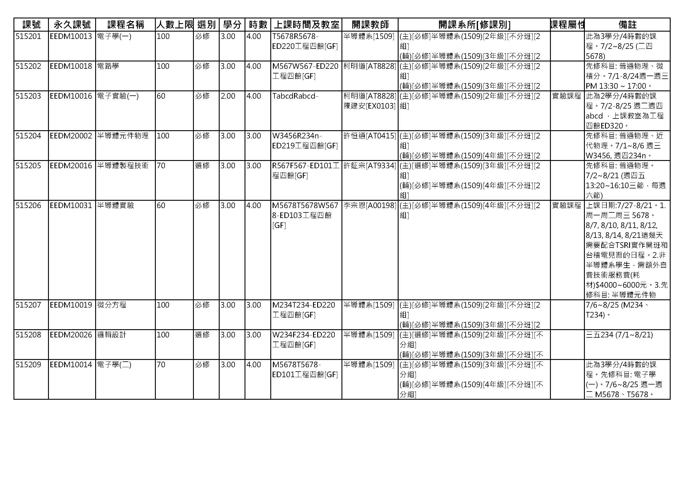
半導體系 [114暑期課程] 開設九門系列課程 (課程名稱: 電路學、邏輯設計、電子學(一)、電子實驗(一)、微分方程、電子學(二)、半導體元件物理、半導體製程技術、半導體實驗),旨在讓學生在不影響學期間常規課程的情況下,利用兩個月的時間密集接觸產業核心知識。授課時間如附件: 114暑課程計劃表。
暑期培育計畫不僅限於陽明交大校內學生,台聯大系統包含清華大學、中央大學與政治大學的學生亦可跨校選修,充分體現學術資源共享的精神。
校方亦鼓勵外系、外校學生善用暑假累積學分,若修讀表現優異,未來可進階申請半導體系的雙主修,在畢業證書上增加專業認可。
114學年度殷之同學長電子實驗獎學金-本系初審榮獲全校第1.3.4名!!
| 名次 | 系級 | 姓名 | 研究專題 | 指導老師 |
| 第 1 名 | 半導體4年級 | 魏庭驊 | Comparative Study of In2O3 and IGZO TFTs with High-k Capping: Enhanced Electrostatics and Thermal Stability of IGZO for M3D integration | 李宗恩教授 |
| 第 3 名 | 半導體3年級 | 羅浩瑋 | 應用於非侵入式神經調控之時頻差干涉刺激器模組化電路實現與驗證 | 柯明道教授 |
| 第 4 名 | 半導體4年級 | 蘇子筌 | Contact Resistance Study in Scaled IGZO TFTs Using Transfer Length Method for 3D DRAM Applications | 李宗恩教授 |
本獎學金經過本校生輔組獎學金委員會初審後,將初審結果送交財團法人竹銘學術基金會複審。
|
|||||||
| 姓名 | 職稱 | 考試名額 | 分機 | 辦公室 | 實驗室 | ||
| 1 | 柯明道 | 教授 | 0 | 31573 | 工程四館644室 | 工程四館307室 | mdker@nycu.edu.tw |
| 2 | 許恒通 | 教授 | 0 | 31985 | 交映樓615室 | 交映樓604室 | hthsu@nycu.edu.tw |
| 3 | 張國恩 | 教授 | 0 | 31884 | 交映樓613室 | 工程五館B42、B43 | gechang@nycu.edu.tw |
| 4 | 王仲益 | 副教授 | 0 | 31695 | 交映樓612室 | 交映樓604室 | cywang72@nycu.edu.tw |
| 5 | 李宗恩 | 助理教授 | 0 | 31635 | 交映樓611室 | 工程五館B42、B43 | telee@nycu.edu.tw |
| 6 | 李義明 | 教授 | 0 | 52974 | 電子資訊中心ES812室 | 電子資訊中心622室 | ymli@nycu.edu.tw |
| 7 | 寒川誠二 | 教授 | 0 | 54623 | 交映樓602室 | 交映樓602室 | seiji.samukawa.e2@nycu.edu.tw |
| 8 | 許鉦宗 | 教授 | 0 | 55805 | 田家炳616室 | 田家炳616室 | sheujt@nycu.edu.tw |
| 數據依系辦公室收到之指導教授協議書作為登記,老師招收學生事宜請與老師討論。 | |||||||
國立陽明交通大學半導體工程學系申請入學
指定項目 第二階段甄試「認識本系及綜合筆試」注意事項
一、甄試日期:115年5月16日(六)
二、甄試地點:國立陽明交通大學光復校區–工程四館B1合勤講堂
三、主要流程:
半導體工程學系分兩個組招生,[奈米科學組] 9:00~12:00 與 [固態電子組] 13:20~16:20 分別進行業界講座、認識本系、師生座談、綜合筆試。
除綜合筆試外,其餘活動皆邀請家長們可一同參與!
[奈米組] 報到 8:30~9:00、[奈米組] 綜合筆試 11:40~12:00
[固態組] 報到 12:50~13:20、[固態組] 綜合筆試 16:00~16:20
四、報到時,請務必攜帶本人身份證件或可證明身份之有照片的健保卡、駕照、護照等,以利查驗。
五、【當日餐盒】均於筆試結束發送,由考生領取 [僅提供考生一份]。
六、【筆試注意事項】試場內除應用文具外,不得攜帶書籍、簿本、電子計算器、電子呼叫器、手機、PDA、電子字典等具有通訊、記憶計算等功能或其他有礙試場安寧、妨害考試公平性之各類物品入座。計時器之鬧鈴功能須關閉。違者送本系系務會議審議。
七、若有任何問題,煩請直接來電 03-5731654。
請備取上的報到同學,參考: 正取生報到注意事項 (繳交附件資料)
115學年度電機工程學系碩士班 半導體組可指導教授名單[隨時更新]
本所將電話通知備取上考生,如電話未能連絡上,將以電子郵件通知考生,但不另行寄發書面遞補錄取通知。
(3/31前) 備取生報到注意事項
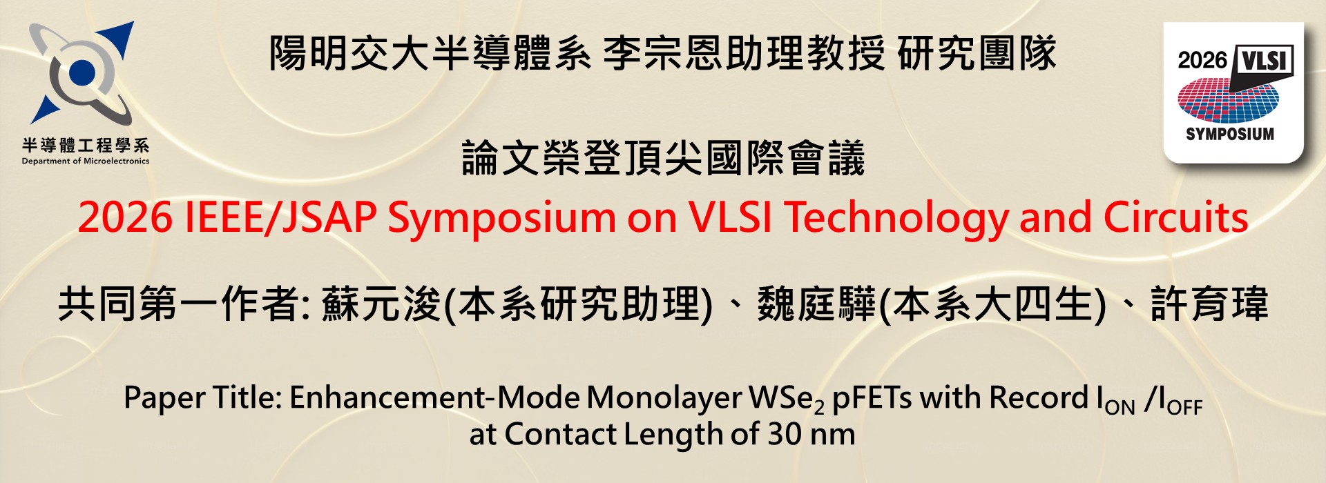
🎉 狂賀!本系研究成果登上國際頂尖會議 🎉
本系李宗恩老師指導之大四學生魏庭驊,其研究成果成功獲選發表於國際頂級會議
IEEE/JSAP Symposium on VLSI Technology & Circuits 2026(VLSI 2026),展現本系在先進半導體領域的卓越研發實力與人才培育成果。
🔬 研究亮點
▪ 本研究聚焦於單層二維材料 WSe₂ 電晶體,在持續微縮趨勢下,仍可同時維持高效能與低漏電特性。
▪ 透過材料工程與接觸工程之創新優化,有效降低接觸電阻並顯著提升元件整體表現。
▪ 研究成果顯示,二維材料電晶體具備成為未來高效能與低功耗晶片關鍵技術之潛力。
🌍 關於 VLSI 國際會議
IEEE/JSAP Symposium on VLSI Technology & Circuits 為微電子與超大型積體電路領域之頂級國際會議之一,每年於美國夏威夷與日本京都輪流舉行,匯聚全球頂尖學術機構與產業領袖,發表最前沿之元件、製程與電路技術,具有高度學術影響力與嚴謹審查機制。
此次由大學部學生以第一線研究成果登上 VLSI 國際舞台,實屬難得,充分展現本系在前瞻半導體技術上的深厚實力與國際競爭力。
👏 再次恭賀李宗恩老師與魏庭驊同學!
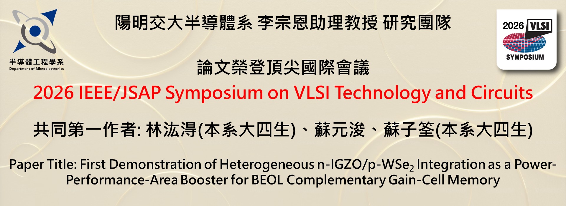
🎉 狂賀!本系再傳捷報 勇登國際頂尖會議 🎉
本系李宗恩老師指導之大四學生林汯淂、蘇子筌,其研究成果成功獲選發表於國際頂級會議
IEEE/JSAP Symposium on VLSI Technology & Circuits 2026(VLSI 2026),再次展現本系在先進積體電路與記憶體技術領域的深厚實力。
🔬 研究亮點
▪ 本研究提出一種可整合於晶片後段(BEOL)的創新增益單元記憶體架構,結合新穎材料技術,兼具高效能與高密度優勢。
▪ 透過反向耦合機制設計,有效抑制元件間干擾,顯著提升讀取穩定性,並兼顧電路設計與系統層級應用之可行性。
▪ 研究成果顯示,此新型記憶體具備應用於未來高效能運算與3D立體堆疊晶片之潛力。
🌍 關於 VLSI 國際會議
IEEE/JSAP Symposium on VLSI Technology & Circuits 為微電子與超大型積體電路領域之頂級國際會議之一,每年於美國夏威夷與日本京都輪流舉行,匯聚全球頂尖學術機構與產業領袖,發表最前沿之元件、製程與電路技術,具高度影響力且審查嚴謹。
本次由大學部學生以創新記憶體架構成果登上國際舞台,實屬難得,不僅展現學生卓越研究能力,更體現本系在前瞻半導體與系統整合領域的國際競爭力。
👏 再次恭賀李宗恩老師、林汯淂與蘇子筌同學!
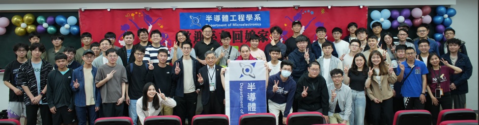
活動:國立陽明交通大學半導體工程學系暨奈米學士班系友回娘家
日期:115年4月11日(六)
時間:12:00~14:00
地點:工程四館117室 [系辦公室106室]
請於4/8(三)前填寫表單: https://forms.gle/kSNEkqSnbw4ayd9s8
回來聚聚聊聊唄~敬備午餐與在校生共享喲~

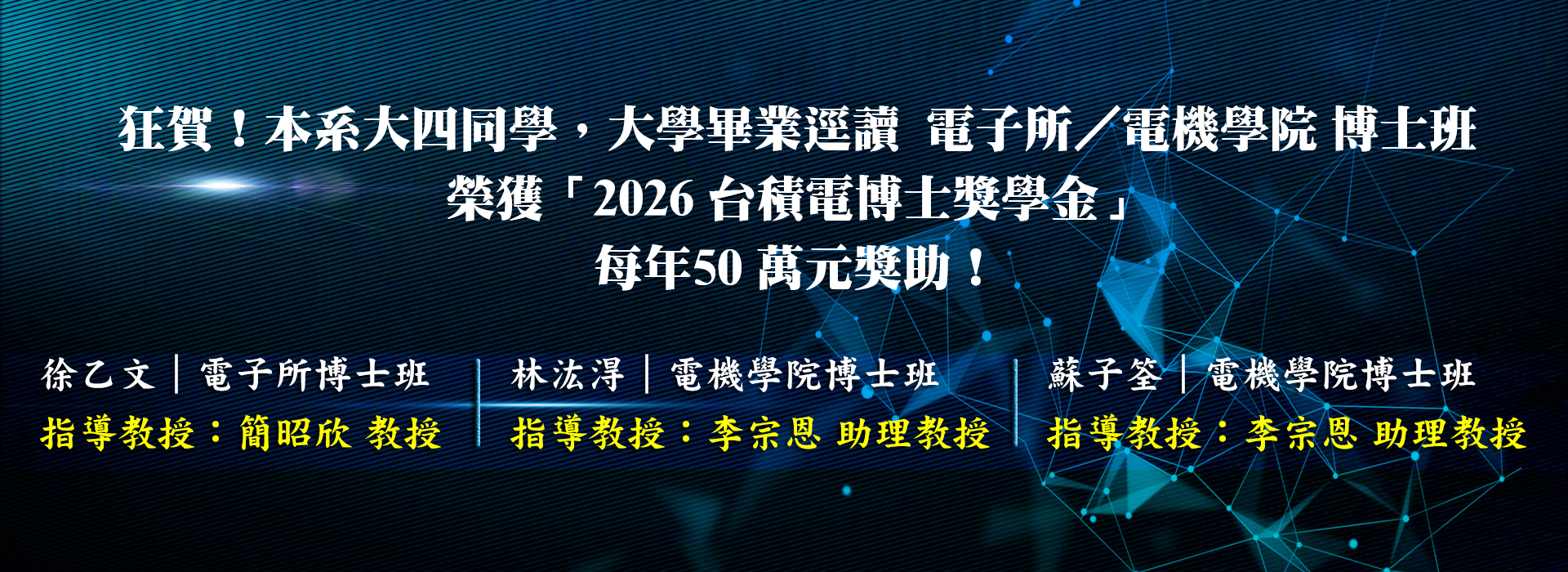
狂賀本系大四同學 大學畢業逕讀 電子所/電機學院 博士班
並在眾多優秀競爭者中脫穎而出,榮獲2026台積電博士獎學金!
徐乙文|電子所博士班
指導教授:簡昭欣 教授
林汯淂|電機學院博士班
指導教授:李宗恩助理教授
蘇子筌|電機學院博士班
指導教授:李宗恩 助理教授