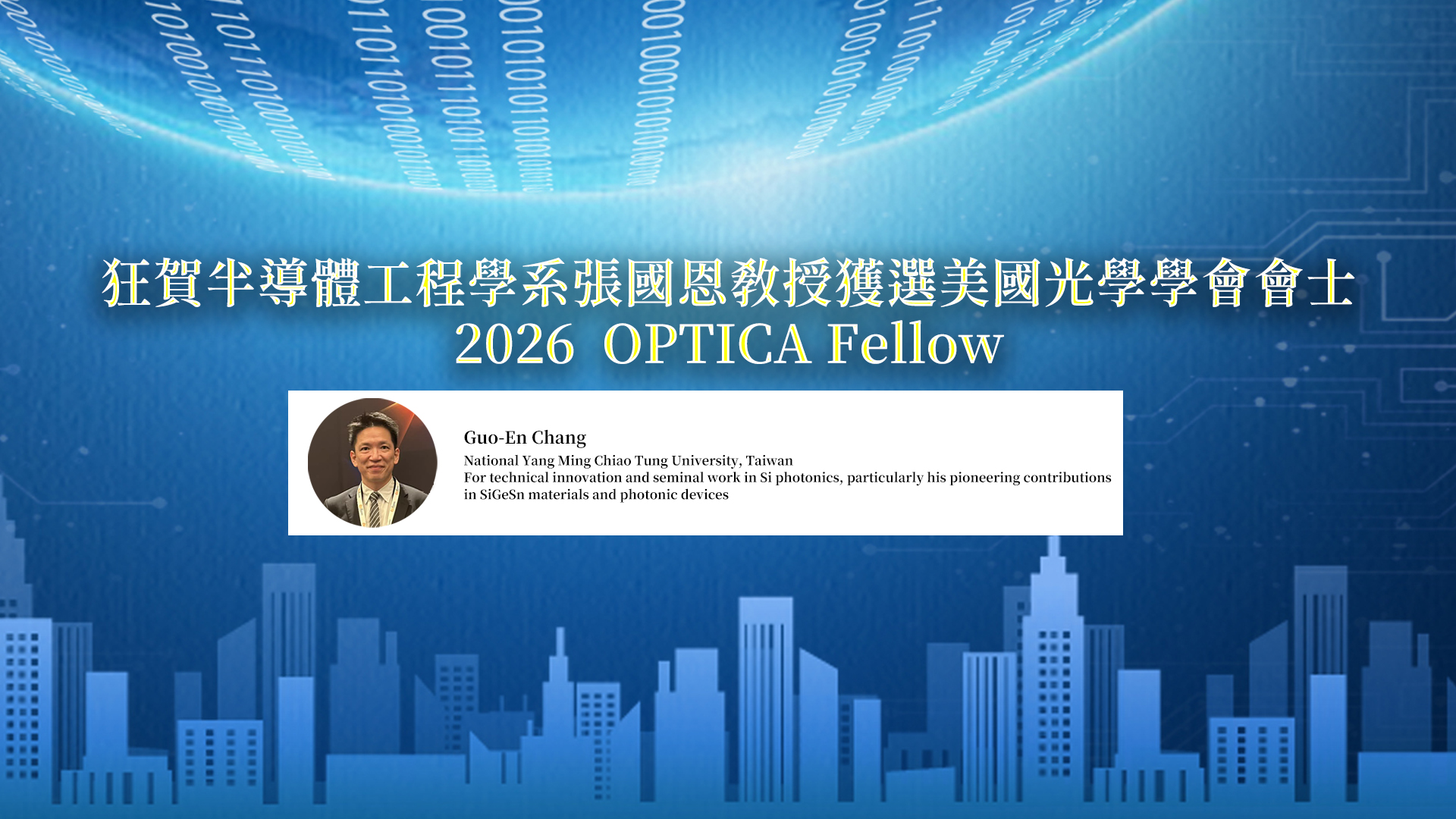
國科會115年度「大專學生研究計畫」開始接受申請(校內至114.2.18止)
一、
二、旨揭計畫國科會線上申請系統校內截止為115年2月22日(
(一)請申請人先行上網註冊,
(二)申請學生之系所主管(或授權系所人員)
(三)請符合資格之申請人於國科會網頁完成線上作業,
三、本案計畫截止日前,恰逢本校年假期間(
四、計畫申請相關文件請至國科會網頁/學術研究/
五、本案校內承辦人員:
(一)計畫業務二組:陳琪惠小姐、許雅如小姐,分機31582、
(二)計畫業務一組:李筱君小姐,分機66058。
二、旨揭計畫國科會線上申請系統校內截止為115年2月22日(
(一)請申請人先行上網註冊,
(二)申請學生之系所主管(或授權系所人員)
(三)請符合資格之申請人於國科會網頁完成線上作業,
三、本案計畫截止日前,恰逢本校年假期間(
四、計畫申請相關文件請至國科會網頁/學術研究/
五、本案校內承辦人員:
(一)計畫業務二組:陳琪惠小姐、許雅如小姐,分機31582、
(二)計畫業務一組:李筱君小姐,分機66058。