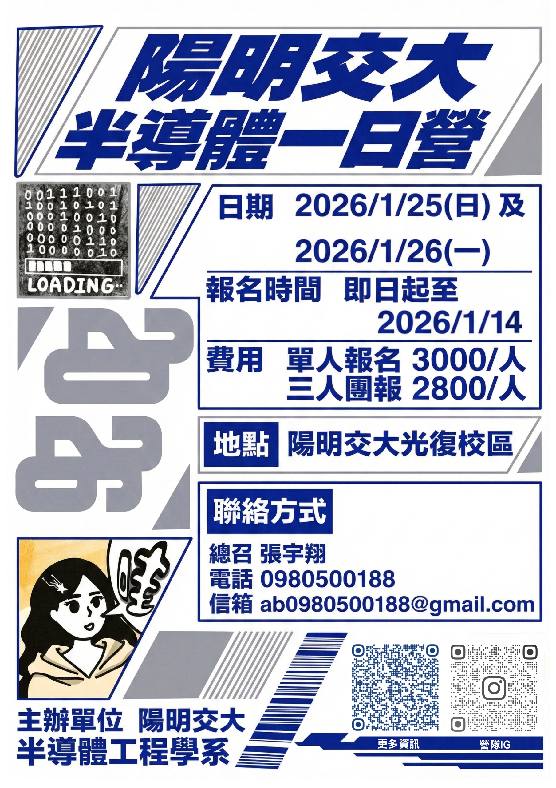
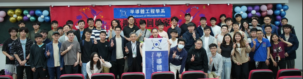
活動:國立陽明交通大學半導體工程學系暨奈米學士班系友回娘家
日期:115年4月11日(六)
時間:12:00~14:00
地點:工程四館117室及106室
回來聚聚聊聊唄~敬備午餐與在校生共享喲~

國科會115年度「大專學生研究計畫」開始接受申請(校內至114.2.18止)
*** You all are welcome to join !!!
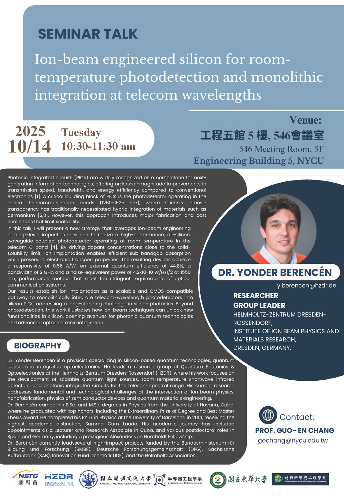
Ion-beam engineered silicon for room-temperature photodetection and monolithic integration at telecom wavelengths
※Speaker :Dr. Yonder Berencen/ Helmholtz-Zentrum Dresden-Rossendorf, Institute of Ion Beam Physics and Materials Research, Dresden, Germany
※Host : Prof. Guo-En Chang 張國恩教授 (Department of Microelectronics)
※Date : 2025-10-14 (Tuesday)
※Time : 10:30~11:30am
※Location :R546, Engineering Building 5, NYCU (GuanFu Campus) 工程五館5樓546室
※Abstract: Photonic integrated circuits (PICs) are widely recognized as a cornerstone for next-generation information technologies, offering orders-of-magnitude improvements in transmission speed, bandwidth, and energy efficiency compared to conventional electronics [1]. A critical building block of PICs is the photodetector operating in the optical telecommunication bands (1260-1625 nm), where silicon’s intrinsic transparency has traditionally necessitated hybrid integration of materials such as germanium [2,3]. However, this approach introduces major fabrication and cost challenges that limit scalability.
In this talk, I will present a new strategy that leverages ion-beam engineering of deep-level impurities in silicon to realize a high-performance, all-silicon, waveguide-coupled photodetector operating at room temperature in the telecom C band [4]. By driving dopant concentrations close to the solid- solubility limit, ion implantation enables efficient sub-bandgap absorption while preserving electronic transport properties. The resulting devices achieve a responsivity of 0.56 A/W, an external quantum efficiency of 44.8%, a bandwidth of 2 GHz, and a noise-equivalent power of 4.2×10⁻¹⁰ W/Hz1/2 at 1550 nm, performance metrics that meet the stringent requirements of optical communication systems.
Our results establish ion implantation as a scalable and CMOS-compatible pathway to monolithically integrate telecom-wavelength photodetectors into silicon PICs, addressing a long-standing challenge in silicon photonics. Beyond photodetection, this work illustrates how ion-beam techniques can unlock new functionalities in silicon, opening avenues for photonic quantum technologies and advanced optoelectronic integration.
***********************************************************************
▼▼▼ 2025 TSMC校園徵才計畫 ▼▼▼
實體|就業博覽會► 2025/03/15(六)
與台積學長姐&HR面對面聊聊,了解不同科系對應到的台積職務、工作型態、學習應用、職涯發展。
親臨現場參與活動,完成履歷投遞即可獲「好禮雙重送」!!!
好禮一|台積電 限量磁吸充電線(數量有限,贈完為止)
好禮二|當日下午抽出 蘋果iPad平板電腦(款式隨機)
線上|徵才說明會► 2025/03/18(二)中文, 03/25(二)日文, 03/27(四)中文, 03/28(五)英文
掌握台積趨勢、職缺資訊及投遞履歷Tips!(線上說明會活動,採事先報名)
活動辦理於中午時段 12 : 15-13 : 15,報名後系統將於活動前1日系統自動寄發活動Teams會議連結。
活動海報:活動海報
線上徵才活動總覽:報名請點我

日本早稻田理工學院說明會
活動資訊:
國科會114年度「大專學生研究計畫」開始接受申請(校內至114.2.18止)
一、依國科會113年12月25日科會綜字第1130088064號函辦理。
二、請申請人先行上網註冊,將歷年成績證明正本掃描成彩色電子檔後上傳,以利辨識,請確認個人基本資料及學術著作資料是否為最新資料,於線上完成相關作業後,將申請案「繳交送出」至就讀系所主管;待系所主管(或授權系所人員)線上「確認」後,再請指導教授於網路上傳「指導教授初評意見表」、勾選「遵照學術倫理規範」並「彙整送出」同意指導;最後由本組上線確認及「彙整送出」,完成線上申請作業。
三、申請學生之系所主管(或授權系所人員)請以各系所之國科會線上申辦系統行政作業帳號及密碼登入,登入後請確認申請人資格是否符合本計畫作業要點第三點之規定,計畫研究期間申請人需為學生身份,並請檢視上傳資料是否完整清晰及申請書表C802內容是否符合以10頁為限(參考文獻不計)之規定。
四、請符合資格之申請人於國科會網頁完成線上作業,由系所單位窗口(於學籍成績管理系統)確認學生在學資格後,列印系統頁面申請人名冊1份(經系所單位主管、一級主管核章)並依序檢附申請人完成學術倫理教育課程訓練至少6小時證明文件,於校內截止收件日前,將上述資料送陽明校區計畫業務一組李筱君小姐;交大校區計畫業務二組陳琪惠、許雅如小姐彙辦。
五、計畫申請相關文件請至國科會網頁/學術研究/補助獎勵辦法及表格/補助專題研究計畫/大專學生研究計畫項下查詢下載,其他注意事項請詳參來文及作業要點說明,或請至國科會網頁「動態資訊」項下「計畫徵求專區」查詢下載(網址: https://www.nstc.gov.tw/ )。